Designing PCBs for Internet of Things (IoT) products, especially those incorporating Ultra-Wideband (UWB) modules, involves a unique set of challenges and considerations. These include ensuring optimal electrical performance, thermal management, mechanical strength, manufacturability, environmental compliance, and cost-effectiveness. This article delves into the specific factors engineers need to consider when designing PCBs for IoT products with UWB modules.
1. Electrical Performance
Signal Integrity
UWB technology relies on transmitting data over very short pulses across a wide frequency spectrum. Ensuring signal integrity in such high-frequency environments is crucial:
- Impedance Matching: Ensure traces have consistent impedance to prevent signal reflections, which is particularly important for high-speed UWB signals.
- Controlled Impedance Traces: Use controlled impedance traces to maintain signal integrity. This requires careful consideration of trace width, spacing, and the dielectric constant of the substrate material.
- Differential Pair Routing: For high-speed UWB signals, use differential pair routing to reduce noise and interference. Ensure the pairs are closely matched in length to avoid skew.
Power Integrity
Maintaining stable power delivery is essential for the reliable operation of IoT devices, especially those with UWB modules:
- Power and Ground Planes: Use dedicated power and ground planes to reduce noise and ensure stable power distribution. This helps in maintaining the integrity of the power supply across the PCB.
- Decoupling Capacitors: Place decoupling capacitors close to the UWB module’s power pins to filter out high-frequency noise.
Electromagnetic Compatibility (EMC)
IoT devices with UWB modules must comply with stringent EMC regulations to prevent interference with other electronic devices:
- Shielding: Implement effective shielding around the UWB module and other sensitive components to prevent electromagnetic interference (EMI). This can involve using metal cans or dedicated ground planes.
- Filter Components: Incorporate EMI filters on power lines and critical signal paths to suppress unwanted noise.
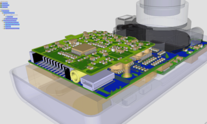
2. Thermal Management
Efficient thermal management ensures the IoT device operates within its safe temperature range, extending its lifespan and reliability:
Thermal Paths
- Thermal Vias: Use thermal vias to transfer heat from high-power components, such as the UWB module, to other layers of the PCB or to a heat sink.
- Copper Thickness: Consider using thicker copper layers to improve heat dissipation.
- Heat Sinks and Pads: Attach heat sinks or thermal pads to high-heat generating components to facilitate heat dissipation.
Thermal Simulation
Conduct thermal simulations to analyze the heat distribution across the PCB. This helps in identifying hotspots and optimizing the placement of thermal vias, heat sinks, and other cooling mechanisms.
3. Mechanical Strength
Mechanical strength is crucial for IoT devices, which are often subjected to various environmental stresses:
Material Selection
- FR-4: A common choice for general applications, providing good mechanical strength and electrical insulation.
- Polyimide: For high-temperature environments, polyimide materials offer superior thermal stability and mechanical strength.
Reinforcement Structures
- Mounting Holes: Strategically place mounting holes to avoid stress concentration and ensure even distribution of mechanical loads.
- Support Structures: Design support structures or stiffeners to enhance the rigidity of the PCB, especially if the device will be exposed to vibration or mechanical shock.
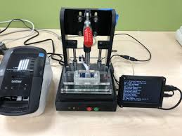
4. Manufacturing Processes
Designing for manufacturability ensures the PCB can be efficiently and reliably produced:
Design for Manufacturability (DFM)
- Minimum Trace Width and Spacing: Adhere to the manufacturer’s minimum trace width and spacing requirements to avoid manufacturing defects.
- Via Sizes and Placement: Ensure via sizes and placements meet the manufacturing capabilities and reliability standards.
Design for Testability (DFT)
Include test points and test paths in the design to facilitate functional testing and troubleshooting. This is particularly important for verifying the performance of the UWB module and other critical components.
5. Environmental Impact and Cost
Balancing environmental impact and cost is essential for the market competitiveness of IoT products:
Environmental Compliance
- Lead-Free Solder: Use lead-free solder to comply with RoHS and other environmental regulations.
- Eco-Friendly Materials: Choose environmentally friendly substrate materials to minimize the environmental impact.
Cost Optimization
- Material Costs: Select materials that balance performance and cost. For instance, using FR-4 can be cost-effective for most IoT applications.
- Manufacturing Costs: Optimize the PCB design to reduce manufacturing steps and material waste, thereby lowering production costs.
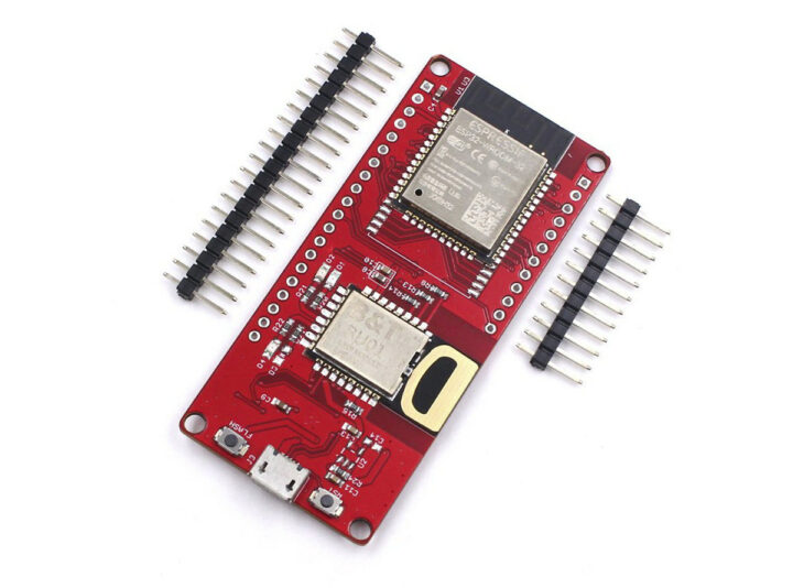
Case Study: PCB Design for an IoT Device with UWB Module
Signal Integrity
- Controlled Impedance Traces: Designed controlled impedance traces for the UWB module to maintain signal integrity.
- Differential Pair Routing: Implemented differential pair routing for UWB signals, ensuring minimal skew by matching trace lengths closely.
Power Integrity
- Dedicated Power and Ground Planes: Used dedicated power and ground planes to ensure stable power delivery and reduce noise.
- Decoupling Capacitors: Placed decoupling capacitors near the UWB module’s power pins to filter out high-frequency noise effectively.
Electromagnetic Compatibility (EMC)
- Shielding: Applied metal shielding around the UWB module to prevent EMI.
- EMI Filters: Incorporated EMI filters on power lines and critical signal paths to suppress unwanted noise.
Thermal Management
- Thermal Vias and Heat Sinks: Used thermal vias and attached heat sinks to high-heat components for efficient heat dissipation.
- Thermal Simulation: Conducted thermal simulations to optimize the placement of thermal management components.
Mechanical Strength
- Material Selection: Chose FR-4 for its good mechanical strength and electrical insulation properties.
- Support Structures: Designed mechanical support structures to enhance the PCB’s rigidity and resistance to mechanical stress.
Manufacturing Processes
- DFM and DFT: Followed DFM guidelines to ensure manufacturability and included test points for easy testing and troubleshooting.
Environmental Impact and Cost
- Lead-Free Solder and Eco-Friendly Materials: Used lead-free solder and eco-friendly materials to comply with environmental regulations.
- Cost Optimization: Balanced material selection and manufacturing steps to minimize costs while maintaining performance.
Conclusion
Designing PCBs for IoT products with UWB modules requires careful consideration of signal integrity, power integrity, electromagnetic compatibility, thermal management, mechanical strength, manufacturability, environmental impact, and cost. By addressing these factors, engineers can ensure their IoT devices perform reliably in various applications, meeting both technical and regulatory requirements. We hope this article helps engineers make informed decisions in their PCB designs, enhancing product quality and market competitiveness.
If you have any questions or need further assistance, please feel free to contact us!