Chinese manufacturer of field effect transistors assembled on PCB.
Fumax is an electronics company that started out as a printed circuit board (PCB) manufacturer in Shenzhen, China, and has many years of experience in circuit board printing and manufacturing.
Shenzhen Fumax Technology Co., Ltd. is a high-tech enterprise engaged in the design, packaging, testing and sales of microelectronic chips. It has excellent technical advantages and efficient service capabilities in PCB articulation, packaging and processing.
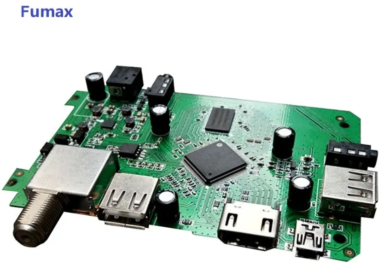
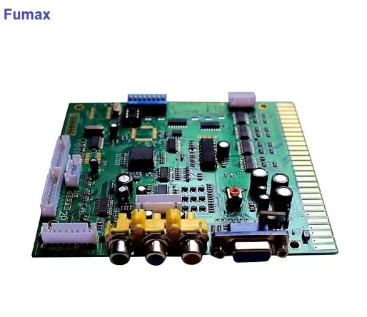
Our one-stop turnkey solutions include component sourcing, PCB manufacturing, PCB assembly, plastic/metal box manufacturing, sub-assembly to fully assembled products. All products are 100% inspected before shipment to ensure they meet customer requirements.
Our R&D services range from new product design, electronic schematic design, PCB layout, mechanical design, prototypes and commissioning to mass production. We have more than 300 highly qualified employees and a total factory size of 5,000 square meters.
Motherboard field effect transistor – packaging form and motherboard technical role
The power supply of motherboards has always been the focus of manufacturers and users, and their attention has shifted from the number of power supply phases to field effect transistor devices. This is because with the advancement of field effect transistor technology, single-chip field effect transistors with high current, small package, and low power consumption and multi-chip DrMOS have begun to be used on motherboards, and new power devices have attracted the attention of motherboard users. This article will briefly introduce the packaging specifications and packaging technology of field effect transistor devices used in motherboards.
After the field effect transistor chip is completed, it needs to be packaged before it can be used. The so-called packaging is to add a shell to the field effect tube chip. This shell has the functions of supporting, protecting, and cooling. It also provides electrical connection and isolation for the chip so that the field effect tube device and other components form a complete circuit.
The material and process of the chip are the decisive factors for the performance and quality of the field effect transistor. Field effect transistor manufacturers naturally focus on the improvement of the chip core structure, density and process to improve the performance of the field effect transistor. These technological improvements will come at a high cost. Packaging technology also directly affects the performance and quality of the chip. Packaging the same chip in different forms can also improve the performance of the chip. Therefore, chip packaging technology is very important.
Distinguished by the way they are installed on the PCB, the packaging forms of power field effect transistors are divided into two categories: through hole and surface mount. The plug-in type means that the pins of the field effect tube pass through the mounting holes of the PCB and are welded to the PCB. Surface mounting is where the field effect tube pins and heat dissipation flange are welded to the pads on the PCB surface.
Common in-line packages include dual in-line packages (DIP), transistor outline packages (TO), pin grid array packages (PGA), etc.
Motherboard field effect tube
Typical surface mount types include transistor outline package (D-PAK), small outline transistor package (SOT), small outline package (SOP), quad flat package (QFP), plastic leaded chip carrier (PLCC), etc.
Motherboard field effect tube
Computer motherboards generally do not use in-line packaged field effect transistors, and this article does not discuss in-line packaged field effect transistors.
Generally speaking, “chip packaging” has two meanings, one is the packaging appearance specification, and the other is the packaging technology. Regarding package appearance specifications, there are international chip packaging standards that stipulate unified package shapes and sizes. Packaging technology refers to the packaging materials and technical processes used by chip manufacturers. Each chip manufacturer has its own technology and registers trademark names for its own technology. Therefore, some packaging technologies have different trademark names, but their technical forms are basically the same. Let’s start with the standard package form factor.
- Standard packaging specifications
1.TO packaging
TO (TransistorOut-line) means “transistor shape” in Chinese. This is an early packaging specification, such as TO-92, TO-92L, TO-220, TO-252, etc., which are all plug-in packaging designs. In recent years, the surface mount market demand has increased, and TO packaging has also progressed to surface mount packaging.
Motherboard field effect tube
TO252 and TO263 are surface mount packages. Among them, TO-252 is also called D-PAK, and TO-263 is also called D2PAK.
The D-PAK packaged MOSFET has three electrodes, gate (G), drain (D), and source (S). The drain (D) pin is cut off and not used. Instead, the heat sink on the back is used as the drain (D), which is directly welded to the PCB. On the one hand, it is used to output large currents, and on the other hand, it dissipates heat through the PCB. Therefore, there are three D-PAK pads on the PCB, and the drain (D) pad is larger.
Motherboard field effect tube
- SOT packaging
SOT (SmallOut-LineTransistor) small outline transistor package. This kind of package is a patch type low-power transistor package, which is smaller than the TO package and is generally used for low-power field effect transistors. Common specifications include: SOT23, SOT89, SOT143, SOT25, etc., and types such as SOT323, SOT363/SOT26 (i.e. SOT23-6) are derived, which are smaller than TO packages.
The SOT-89 field effect transistor with four terminal pins is commonly used on motherboards.
Motherboard field effect tube
- SOP packaging
SOP (Small Out-Line Package) means “small outline package” in Chinese. SOP is one of the surface mount packages. The pins are led out from both sides of the package in a gull wing shape (L shape). The materials are plastic and ceramic. SOP is also called SOL and DFP. SOP packaging standards include SOP-8, SOP-16, SOP-20, SOP-28, etc. The number after SOP indicates the number of pins. Most SOP packages of field effect transistors adopt SOP-8 specifications. The industry often omits the “P” and calls it SO (Small Out-Line).
Motherboard field effect tube
SO-8 is packaged in plastic, has no heat dissipation bottom plate, and has poor heat dissipation. It is generally used for low-power field effect tubes. SO-8 was first developed by PHILIP Company, and later gradually derived standard specifications such as TSOP (Thin Small Outline Package), VSOP (Very Small Outline Package), SSOP (Shrink SOP), TSSOP (Thin Shrink SOP), etc. Among these derived packaging specifications, TSOP and TSSOP are commonly used in field effect transistor packaging.
Motherboard field effect tube
- QFN-56 package
QFN (Quad Flat Non-leaded package) is one of the surface mount packages. It is called quad flat non-leaded package in Chinese. It is an emerging surface mount chip packaging technology with small pad size, small volume and plastic as sealing material. . Now it is often called LCC. QFN is the name specified by the Japan Electronics Machinery Industries Association. There are electrode contacts on the four sides of the package. Since there are no leads, the mounting area is smaller than QFP and the height is lower than QFP. This kind of packaging is also called LCC, PCLC, P-LCC, etc. QFN is originally used for packaging of integrated circuits, and field effect transistors will not be used. The DrMOS proposed by Intel that integrates drivers and field effect transistors is packaged in QFN-56. 56 means there are 56 connection pins on the back of the chip.