Wireless module PCB assembly manufacturer – WiFi PCB design OEM/ODM
The following are some companies engaged in WiFi module PCB assembly, wireless module PCB design, and WiFi module circuit design:
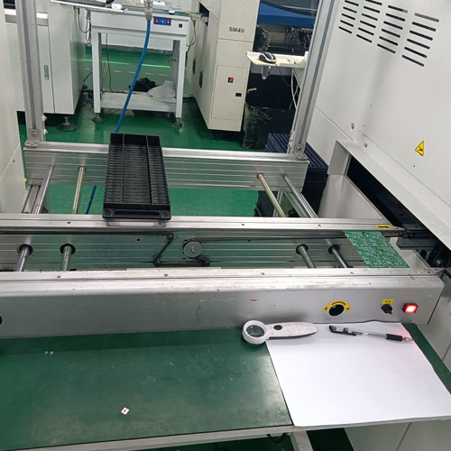
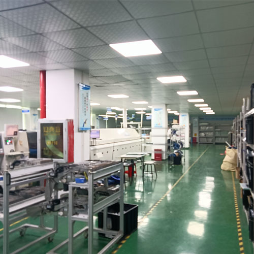
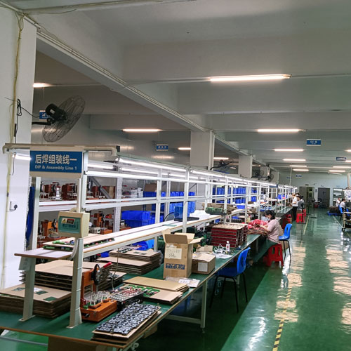
- Shenzhen Fumax Technology Co., Ltd. focuses on one-stop services such as wireless module PCB assembly, WiFi circuit board design and custom development, software programming, SMT patching, DIP welding, WiFi PCB assembly testing and painting.
The production base is located in Fuyong, Baoan District, Shenzhen City, and the office is located in Nanshan District, Shenzhen City.
Fumax Technology provides diversified OEM and ODM services to domestic and foreign customers. We help customers solve operational problems such as WiFi module PCB circuit board design, mechanical or electronic design, sample and mass production, service and logistics, etc., so that customers can focus on front-end high-value businesses such as sales and R&D, marketing and branding, and help customers obtain Continuous great success is the core value of all colleagues at Fumax Technology.
Fumax’s products involve industrial control, vehicle systems, MCUs, remote communications, smart homes, medical equipment and consumer electronics and other fields! Products are sold in many countries around the world!
- Broadcom: The world’s leading wired and wireless communications semiconductor company, providing a wide range of system-on-chip and software solutions.
- Hailingke: A technology-based enterprise that specializes in R&D, production and sales of IoT smart home WIFI module products. It was founded in September 2009.
- Lierda: A high-tech enterprise that provides embedded technology solutions for the Internet of Things. It is headquartered in Hangzhou, a world-famous tourist city, with a registered capital of 56.67 million yuan.
- USI Electronics Co., Ltd. (USI): Mainly produces EMS, JDM, and ODM for high-end electronic products such as information, communications, consumer electronics, and automotive electronics. Its main products include WiFi ADSL, WiMAX, WiFi AP, WiFi Module, etc.
- Shenzhen Bopengfa Electronic Technology Co., Ltd.: a high-tech enterprise specializing in wireless Internet-related radio frequency series module application solutions and product comprehensive solution platforms.
- AzureWave: Core WiFi chips used: Marvell, Broadcom, Qualcomm Atheros, MTK Ralink.
- Broadlink: It is affiliated to Hangzhou Gubei Electronic Technology Co., Ltd. and uses core WiFi chips: Marvell, MTK, etc.
The above companies are all companies with certain strengths in the electronics industry. Which company to choose depends on needs and conditions.
PCB layout and routing considerations for WIFI and BT
- When laying out the overall module layout, the WIFI module should be kept as far away from DDR, HDMI, USB, LCD circuits and speakers as possible interference modules or connection sockets;
- The layout of the crystal circuit needs to be given priority. The layout should be on the same layer as the chip and placed as close as possible to avoid drilling holes. The crystal traces should be as short as possible, away from interference sources, and as far away as possible from the antenna area; the crystal and clock signals need to be fully covered. For ground processing, add at least one GND via every 100 mil to the ground wire, and ensure that the ground reference plane of the adjacent layer is complete.
- Route the 32.768k wire separately and cover it with ground, and add at least one GND via every 400 mil of the ground wire;
- When the VBAT power supply is working, the circuit is large, the single antenna module is more than 600mA, and the entire main power supply circuit must be more than 20mil. The trace span of the access pin is the same width as the PIN pin. If you need to drill at least two vias; VBAT The power supply decoupling capacitor must be close to the module power pin and isolated from the adjacent crystal clock trace by a ground wire of about 10 mil.
- The antenna matching circuit must be close to the antenna base, and the antenna wiring must be 50 ohms (it can be used as a reference for the interlayer according to the actual stacking conditions) to ensure the integrity of the reference ground. No other signal lines or power supplies are allowed below;
- The longer the antenna wiring, the greater the energy loss. Therefore, when designing, the shorter the antenna path, the better. There should be no branches and try not to change layers. More ground vias need to be drilled around the antenna. If there are any requirements for the antenna wiring, When turning, you cannot use the corner method, and you need to use arc routing.
- If it is a 2X2 MIMO antenna interface, the outlet direction between the two antenna ports needs to consider the position of the two antennas. The positions of the two antennas need to be as far away as possible to avoid interference, and vertical placement should be considered to avoid mutual interference.
- When laying out the inductor of the module, please note that after the wiring comes out of the inductor, it first passes through the capacitor and then enters the module power pin. Keep the first layer under the module intact and do not have other signal traces.
- The six traces of SDIO_D0-D3, SDIO-CMD and SDIO_CLK should be parallel and equal in length as much as possible. The difference in trace length should be controlled within ±25mil, and the adjacent layers should be kept away from other power supply and clock traces. SDIO_CLK needs to be handled throughout the whole process.
Shenzhen Fumax Technology Co., Ltd. provides PCB layout and wiring and wireless module circuit design solutions for WIFI and Bluetooth (BT).