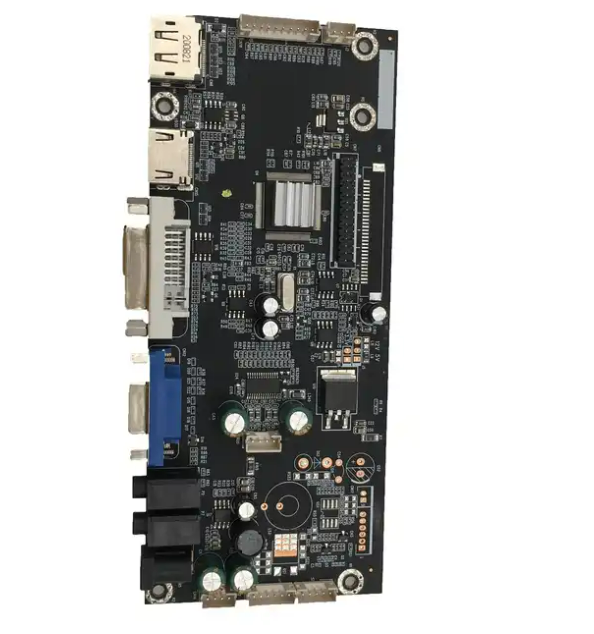
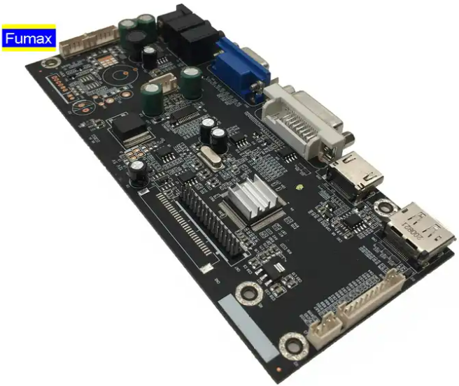
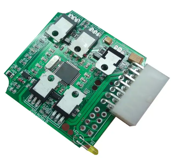
PCB MCU assembly testing is to test the electrical performance and functionality of the assembled PCB board to ensure that each component is working properly and the circuit design meets the requirements.
The MCU development process is from MCU prototype design to prototype testing. The testing content covers many aspects such as power supply stability, signal integrity, functional module performance, and environmental adaptability.
Through testing, potential problems can be discovered and corrected, improving product reliability and stability.
- Do MCU PCB assembly manufacturers need to conduct EMC testing?
- PCB MCU (Microcontroller Unit) assembly manufacturer EMC testing process
- EMC basics of PCB (Printed Circuit Board) design and layout
- What functions need to be tested in MCU system design?
- Testing of the PCB board of the smallest Microcontroller system
Fumax provides ultra-low power MCU, motor control MCU, general control MCU, automotive electronic MCU, industrial and other electronic design, controller module PCB customization and design services, professional electronic circuit layout, and PCB assembly factory.
Do MCU PCB assembly manufacturers need to conduct EMC testing?
Yes, MCU PCB assembly manufacturers need to do EMC testing.
EMC testing includes two parts: electromagnetic interference (EMI) and electromagnetic susceptibility (EMS). MCU PCB assembly manufacturers need to ensure that their products meet the limit value requirements and immunity requirements stipulated in relevant standards before leaving the factory. The test environment needs to meet certain requirements. For example, the test site should have a shielded room or an anechoic room.
PCB MCU (Microcontroller Unit) assembly manufacturer EMC testing process
The EMC testing of MCU PCB assembly manufacturers mainly includes electromagnetic interference (EMI) and electromagnetic susceptibility (EMS).
- EMI test: Test the intensity of electromagnetic interference sent by MCU PCB assembly products to the outside world to ensure that it meets the limit value requirements stipulated in relevant standards. This includes testing for electromagnetic radiated emissions, conducted emissions, etc.
- EMS test: Test the sensitivity of MCU PCB assembly products under electromagnetic environmental conditions that specify electromagnetic disturbance intensity to ensure that they meet the immunity requirements stipulated in relevant standards. This includes testing for surge, static electricity, radiated immunity, etc.
In order to ensure the accuracy and reliability of test results, electromagnetic compatibility measurement has high requirements on the test environment. The measurement sites include outdoor open fields, shielded rooms or anechoic chambers, etc. During the EMC testing process, MCU PCB assembly manufacturers need to design and manufacture in accordance with relevant standards and specifications to improve the electromagnetic compatibility performance and reliability of the product.
EMC basics of PCB (Printed Circuit Board) design and layout
EMC basic knowledge of PCB (Printed Circuit Board) design and layout includes the following aspects:
- Electromagnetic compatibility (EMC) concept: Electromagnetic compatibility means that electronic equipment can work normally in various electromagnetic environments without causing excessive interference to other equipment. In PCB design and layout, it is necessary to consider how to reduce the electromagnetic interference (EMI) of the device itself while improving its resistance to external electromagnetic interference.
- EMC standards and specifications: When designing PCBs, you need to refer to relevant EMC standards and specifications, such as those set by organizations such as the International Electrotechnical Commission (IEC) and the U.S. Federal Communications Commission (FCC). These standards and specifications specify electromagnetic emissions and immunity requirements for electronic equipment.
- PCB layout: During the PCB layout stage, it is necessary to consider how to reasonably arrange the position and direction of components to reduce electromagnetic radiation and improve immunity. For example, keep high-speed signal lines as close as possible, lay out analog circuits and digital circuits separately, etc.
- Layer design: The layer design of PCB is critical to EMC performance. Reasonable layer layout can reduce interference between signals and improve signal quality. For example, the power layer and signal layer should be closer to reduce interference between power and signal.
- Signal integrity: Signal integrity means that the signal is not distorted or has a small error during transmission. In order to improve signal integrity, it is necessary to consider how to reduce interference factors such as signal reflection, crosstalk, and ground bounce in PCB design. For example, adding some decoupling capacitors around high-speed signal lines can reduce noise interference.
- Power supply and ground design: Power supply and ground are two very important factors in PCB design. Good power supply and ground design can reduce noise interference between power supply and ground, while improving the immunity of the equipment. For example, multiple power planes can be used to reduce noise interference between power and ground.
- Component selection and layout: Component selection and layout also have a great impact on the EMC performance of PCB. When selecting, you need to consider the electromagnetic compatibility performance and reliability of the components; when laying out, you need to consider how to reasonably arrange the location and direction of the components to reduce electromagnetic radiation and improve immunity.
In short, many factors need to be considered in PCB design and layout to improve the electromagnetic compatibility performance of the device. These factors include reasonable layout, good power and ground design, signal integrity considerations, component selection and layout, etc. Only by comprehensively considering these factors can we design a PCB that meets EMC standards.
What functions need to be tested in MCU system design?
Functions that need to be tested in MCU system design include but are not limited to:
- Performance test: Test whether the performance indicators of the MCU meet the design requirements, such as clock frequency, data transfer rate, memory read and write speed, etc.
- Reliability testing: Test the MCU for long periods of time or repeatedly under simulated extreme environmental conditions to discover possible potential problems, including ESD, EFT, temperature testing, etc.
- Compatibility test: Test the compatibility of the MCU with other devices to ensure that the MCU can seamlessly connect with other devices and complete specified tasks.
Testing of the PCB board of the smallest Microcontroller system
The test of the PCB board of the minimum microcontroller system mainly includes the following steps:
- Prepare test equipment: Test equipment includes power supply, multimeter, oscilloscope, etc.
- Connect the circuit: Connect the PCB board of the minimum microcontroller system to the power supply, multimeter, oscilloscope and other equipment.
- Power supply test: Turn on the power and observe whether the power supply is stable and whether there are abnormal noise or fluctuations. Use a multimeter to test whether the power supply voltage is within the specified range.
- Signal test: Use an oscilloscope to test whether the signal waveform is correct in different parts of the PCB board. Parameters such as amplitude, frequency and phase of the signal can be observed.
- Functional test: Through programming and debugging, make the microcontroller minimum system run and test whether its function is normal. Each functional module can be tested one by one, such as I/O ports, timers, serial communication, etc.
- Boundary condition testing: Test the performance and reliability of the smallest microcontroller system under extreme conditions, such as temperature, humidity, and voltage.
- Safety test: Test the PCB board for problems such as electromagnetic interference, overheating or short circuit to ensure the safety and stability of the system.
- Performance test: Test the performance indicators of the minimum microcontroller system, such as processing speed, memory read and write speed, etc.
- Fault diagnosis and troubleshooting: When a fault occurs, use troubleshooting methods to identify the cause of the fault one by one and repair the problem.
- Recording and analysis: Record the data and analysis results during the test process to facilitate subsequent summary and improvement.
Through the above steps, the PCB board test of the minimum Microcontroller system can be completed to ensure the normal operation and reliability of the system.