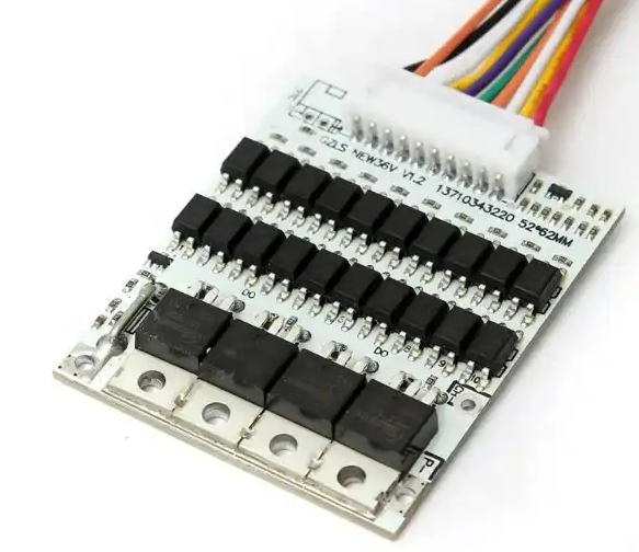
As the electric vehicle market continues to expand, the performance and safety of the automotive battery management system (Battery Management System, BMS), as a key component, are crucial.
PCB (Printed Circuit Board), as the core component of BMS, is responsible for connecting and transmitting battery data. Therefore, high-quality PCB assembly is crucial to ensure stable operation of the battery management system.
This article will introduce in detail the entire process of automotive battery management system PCB assembly, including design, material selection, manufacturing, assembly and testing.
Automobile battery management system PCB design
Before starting PCB assembly, detailed design work first needs to be done. The following factors should be considered during the design phase:
- Determine the size and shape of the circuit board to meet the vehicle interior space constraints and layout requirements.
- According to functional requirements, determine the type and quantity of components on the circuit board, as well as the connection methods between components.
- Select the appropriate circuit board material and number of layers to meet the mechanical strength, heat resistance, insulation and other requirements in the automotive environment.
- Design reasonable wiring rules to ensure the correctness and reliability of the circuit.
- Consider the convenience of testing and maintenance, and design appropriate interfaces and test points.
After completing the design, detailed circuit board drawings should be generated, including component layout diagrams, wiring diagrams, component lists, etc.
material selection
When selecting the materials required for PCB assembly, the following factors should be considered:
- Circuit board material: Select the appropriate circuit board material according to the application environment and reliability requirements, such as FR4, CEM-1, etc.
- Components and connectors: Select appropriate resistors, capacitors, transistors and other components according to the circuit design, as well as connectors, sockets and other connecting devices.
- Auxiliary materials: including solder, adhesives, insulation materials, etc., high-quality products that meet standard requirements should be selected.
BMS PCB manufacturing
The PCB manufacturing stage involves transferring the circuit pattern to the circuit board substrate, followed by processing processes such as etching and drilling. The main steps in this phase include:
- Prepare circuit board substrate: Prepare the corresponding substrate according to the selected circuit board material.
- Print circuit graphics: Print the designed circuit graphics onto the circuit board substrate.
- Transfer and positioning: Ensure that the circuit pattern is correctly transferred to the substrate and positioned accurately.
- Processing and manufacturing: Perform necessary processing and manufacturing steps, such as etching, drilling, electroplating, etc., to form conductive traces and connection holes required for circuit and component installation.
- Quality inspection: Strict quality inspection is carried out throughout the manufacturing process to ensure that each step meets the design requirements and quality control standards.
- Final inspection: After completing all manufacturing steps, a final quality inspection is performed to ensure that the performance and quality of the circuit board meet the requirements.
BMS PCB assembly
PCB assembly is the process of soldering or assembling electronic components onto a printed circuit board. The main steps in this phase include:
- Component preparation: Prepare the required electronic components according to the circuit design, and perform necessary testing to ensure their quality and reliability.
- Soldering: Solder the components to the printed circuit board using a suitable soldering process. During the welding process, ensure that the components are arranged neatly and the quality of the welding points is reliable.
- Assembly: After welding is completed, perform necessary assembly steps, such as installing accessories such as shells and radiators. Make sure all components are installed correctly and secured in place.
- Debugging and testing: Carry out preliminary debugging and testing after the assembly is completed to check whether the basic functions of the printed circuit board are normal. Testing should include measurement and analysis of power supply voltage, signal integrity, temperature and other parameters.
- Final inspection: After completing all tests, conduct a final quality inspection to ensure that the performance and quality of the printed circuit board meet the requirements.
- Packaging and transportation: Properly package and protect the finished product according to actual needs to ensure that it will not be damaged during transportation. At the same time, the product name, specifications, quantity and other relevant information should be marked to facilitate subsequent warehousing and logistics management.
- Documentation: Detailed documentation should be maintained throughout the entire assembly process, including production plans, process flows, test reports, etc. These records are very valuable for subsequent product maintenance and problem tracing.
- Environmental control: During the PCB assembly process, attention should be paid to controlling environmental factors such as the temperature and humidity of the working environment to ensure that it meets process requirements and product quality standards. In addition, the cleanliness of the workplace should be maintained to avoid dust and other contaminants from affecting product quality.
- Personnel training and safety: Provide necessary training to personnel involved in PCB assembly to ensure that they are familiar with operating procedures, master relevant skills and safety knowledge. At the same time, necessary safety protection measures should be provided, such as wearing protective glasses, gloves, etc., to ensure the safety and health of personnel.
- Continuous improvement and optimization: Through the monitoring and analysis of the production process, we will continue to discover existing problems and room for improvement, continue to optimize the process flow and management system, and improve production efficiency and product quality levels.
At the same time, attention should be paid to industry dynamics and technological development trends, and timely introduction of new technologies and new processes to improve product competitiveness. Through the implementation of these measures, the efficiency and quality level of PCB assembly can be continuously improved.