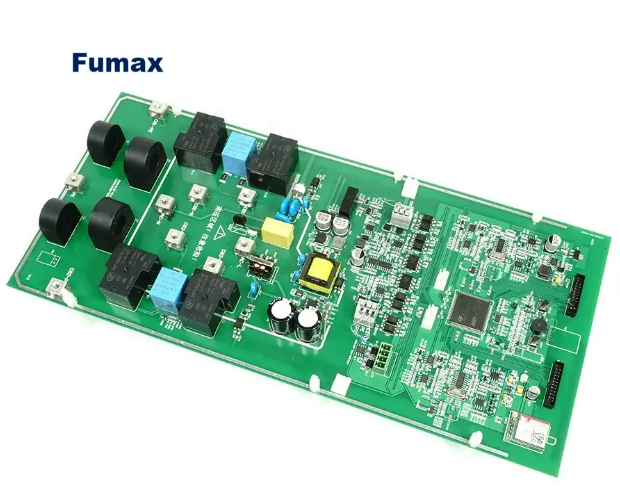
In the production process of Brazilian PCB light board, silk screen printing process is a widely used technology.
The silk screen process plays an important role in the manufacturing of PCB boards in Brazil. It can achieve high-precision and high-definition printing effects to meet various product needs.
First of all, the application of silk screen printing technology in Brazilian PCB light board manufacturing has various advantages.
The silk screen printing process has a high printing resolution and can print very fine patterns and text, which is crucial for PCB light boards that require high-definition printing effects. In addition, the silk screen printing process has fast printing speed, which can achieve efficient production and reduce production costs.

At the same time, the ink or photosensitive material used in the screen printing process has good adhesion and durability, which can ensure that the printed content remains clear and stable for a long time.
In the screen printing process of Brazilian PCB light board, the following key steps are mainly involved:
- Screen production: First, you need to make a screen as a template for printing. The mesh size and mesh density of the screen need to be selected according to the printing requirements to ensure the accuracy and effect of printing.
- Selection of ink or photosensitive material: Select the appropriate photosensitive ink or photosensitive material according to the material and printing requirements of the PCB light board. These materials need to have good adhesion and durability to ensure that the printed content remains clear and stable for a long time.
- Preparation work before printing: The PCB light board needs to be pre-processed before printing, such as cleaning, coating, etc., to ensure that the ink or photosensitive material can adhere well to the PCB light board during printing.
- Printing: Fix the screen on the printing machine, adjust the angle and pressure of the scraper, then pour the ink or photosensitive material into the screen, use the scraper to scrape the ink or photosensitive material flat on the screen, and then put the PCB light board (board ) is placed on the workbench of the printing machine, so that the screen and PCB board are closely attached, and printed with a scraper.
- Drying and curing: After printing is completed, the ink or photosensitive material needs to be dried and cured so that they can be fully dried and fixed on the PCB board.
- Testing: Finally, the printing quality needs to be tested to check whether the printing clarity, position, color, etc. meet the requirements.
In addition to the silk screen printing process, other processes may also be used in the manufacturing of Brazilian PCB boards, such as inkjet printing, labeling machines, etc. Each of these processes has its own characteristics and can be selected according to specific product requirements and production conditions.
In the screen printing process of Brazilian PCB light boards, there are also some special application forms, such as three-dimensional screen printing and functional screen printing. Three-dimensional silk screen printing can print three-dimensional patterns and text on the PCB board to increase the visual effect and touch of the product. Functional silk screen printing can print materials or components with special functions on the PCB board, such as conductive glue, sensors, etc., to achieve more functions and applications.
In addition, with the continuous advancement of technology and the growing demand for applications, the screen printing process of Brazilian PCB light boards is also constantly innovating and improving. New screen printing equipment and materials are constantly emerging, providing more choices and possibilities for the manufacturing of PCB light boards.
For example, high-precision screen printing equipment and automated production lines can improve production efficiency and product quality; new photosensitive inks and photosensitive materials can improve printing clarity and adhesion; intelligent testing equipment can realize real-time monitoring and control of printing quality .
In general, the silk screen printing process has broad application prospects in Brazilian PCB light board manufacturing.
Through continuous technological innovation and application expansion, the screen printing process will continue to exert its advantages and provide more possibilities for Brazilian PCB light board manufacturing.