The sensor PCB principle design solution aims to provide a stable, reliable and efficient design for the sensor circuit.
This article will introduce the basic steps of sensor PCB principle design, including demand analysis, hardware selection, schematic design, PCB layout, PCB wiring, PCB verification and testing.
Demand analysis
Before carrying out the sensor PCB principle design scheme, you first need to understand the specific application scenarios, performance requirements, working environment, etc. of the sensor. By analyzing the requirements, the basic parameters of the PCB board can be determined, such as size, number of layers, materials, etc. At the same time, the maintainability, repairability and reliability of the PCB board also need to be considered.
Hardware selection
Based on the demand analysis results, select appropriate hardware devices, including sensors, chips, power supplies, capacitors, resistors, etc. When selecting hardware, you need to consider its performance parameters, reliability, price and other factors. At the same time, the maintainability and replaceability of hardware equipment also need to be considered.
PCB sensor schematic design
After the hardware selection is completed, schematic design needs to be carried out. Schematic design is the core of the sensor PCB principle design plan, which determines the working principle and connection method of the entire circuit. When designing a schematic, the following factors need to be considered:
- Circuit stability: Ensure that the circuit works stably under various conditions without noise or interference.
- Circuit reliability: Choose reliable components and connection methods to ensure the long-term stability and life of the circuit.
- Circuit maintainability: Ensure that each part of the circuit is easy to maintain and repair, and it is convenient to replace components.
- Circuit scalability: Consider possible future upgrades or expansion needs to accommodate future development.
Sensor PCB layout
After the schematic design is completed, PCB layout needs to be carried out. PCB layout is an important part of the sensor PCB principle design plan, which determines the overall structure and use effect of the PCB board. When doing PCB layout, you need to consider the following factors:
- Arrangement of devices: Arrange the arrangement of devices reasonably according to the working principle and signal flow of the circuit.
- Spacing of devices: Ensure that the spacing between devices is reasonable to avoid signal interference and thermal interference.
- Distribution of power supply and ground wires: Reasonably distribute power supply and ground wires to reduce the resistance and inductance between power supply and ground wires.
- Thermal design: Carry out a reasonable thermal design based on the operating temperature and heat dissipation requirements of the device.
PCB layout
After the PCB layout is completed, PCB routing needs to be performed. PCB wiring is a key link in the sensor PCB principle design scheme, which determines the performance and reliability of the circuit. When doing PCB routing, you need to consider the following factors:
- The direction of the signal line: According to the working principle and signal flow of the circuit, reasonably arrange the direction of the signal line.
- The direction of the power supply and ground wires: Reasonably arrange the direction of the power supply and ground wires to ensure the stability and reliability of the power supply and ground wires.
What is the checksum test in the sensor PCB principle design solution?
In the sensor PCB principle design scheme, verification and testing are important links to ensure design quality and reliability.
- Verification: In the verification stage, the PCB principle design plan needs to be carefully inspected and verified. This includes checking whether the schematic is designed correctly, whether the PCB layout and wiring are reasonable, and whether the connections of various devices are correct. During the verification process, attention needs to be paid to the stability, reliability, maintainability and scalability of the circuit to ensure that the design solution meets the needs.
- Testing: Testing is an important means to verify the actual performance of PCB principle design solutions. During the testing phase, the sensor PCB needs to be physically operated and tested to verify its performance and reliability. This includes testing the sensor’s accuracy, sensitivity, response speed and other performance indicators, as well as testing the stability and durability of the PCB. Through testing, potential problems can be discovered and solved in time to ensure the stability and reliability of the sensor PCB in practical applications.
Verification and testing are an indispensable part of the sensor PCB principle design scheme. They help ensure the accuracy and reliability of the design and provide strong guarantee for practical applications.
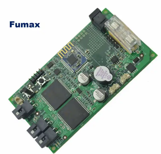
PCB sensor manufacturer
Fumax PCB sensor manufacturer is committed to providing high-quality, high-precision PCB sensor solutions. We have a professional R&D team and advanced production equipment to ensure that each product undergoes strict quality control. Our products are widely used in various fields, such as industrial automation, medical equipment, automotive electronics, etc. We take innovation as our driving force and continuously improve our technical level to meet the changing needs of our customers. Choose us and you will get stable, reliable and efficient PCB sensor solutions.