Sensor PCB circuit module project design involves integrating sensor elements with PCB circuit boards to achieve specific detection functions.
This design needs to take into account the collection, processing and output of sensor signals, as well as the layout and wiring of the PCB circuit board to ensure signal stability and reliability.
In addition, the sensor PCB circuit module project design also needs to consider requirements such as anti-interference performance, temperature stability, accuracy and linearity to ensure the performance and quality of the entire system.
Project Overview
This project aims to design a PCB circuit module for detecting and transmitting sensor signals. The module will feature high sensitivity, low noise, long-term stability and reliability, making it suitable for a variety of sensor applications. Project requirements include circuit board design, component selection and layout, signal processing and transmission, power management, etc.
Project needs analysis
- Sensor signal collection: The circuit module must have the ability to accurately collect sensor signals, including analog signals and digital signals.
- Signal processing and transmission: Perform necessary processing on the collected signals, such as amplification, filtering, AD conversion, etc., and transmit them to the host computer through the serial port or network.
- Power management: Reasonably manage power, reduce power consumption, and improve battery life.
- Reliability: Circuit modules need to have high stability and reliability to adapt to various environmental conditions.
- Maintainability: Convenient for debugging and maintenance, and easy to replace faulty components.
Sensor circuit design
- Power circuit: Use linear voltage regulator or switching power supply to provide stable voltage and current.
- Signal acquisition circuit: Select appropriate amplifiers, filters and other components according to the sensor type to achieve accurate signal acquisition.
- Signal processing circuit: Perform necessary processing on the collected signals, such as amplification, filtering, AD conversion, etc.
- Transmission circuit: Use serial port or network interface to transmit the processed signal to the host computer.
- Protection circuit: Set up protection measures to prevent overvoltage, overcurrent and other abnormal conditions from causing damage to the circuit.
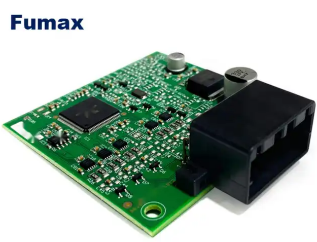
Sensor PCB design
- Component layout: Reasonably arrange component locations to ensure short signal paths and low interference.
- Power supply wiring: Reasonably plan the power supply lines to reduce power supply noise interference.
- Signal wiring: Choose appropriate wire materials and widths to reduce signal transmission loss and interference.
- Thermal design: Reasonably design the heat dissipation device to ensure that the circuit module works normally in high temperature environments.
- Manufacturing process: Choose appropriate manufacturing processes, such as multi-layer boards, FPC, etc., to improve the stability and reliability of the circuit module.
Sensor board testing and verification
- Functional test: Functionally test the circuit module to ensure that each function is implemented normally.
- Performance test: Test the main performance indicators of the circuit module, such as sensitivity, resolution, stability, etc.
- Environmental adaptability test: The circuit module is tested under different environmental conditions to ensure that it can adapt to various environmental conditions.
- Reliability test: Carry out long-term operation and repeated power-on and off tests to verify the reliability and stability of the circuit module.
- Fault diagnosis and troubleshooting: Diagnose and troubleshoot faults to improve the repairability and maintainability of circuit modules.
Project summary and optimization suggestions
- Project summary: summarize the entire project and analyze the results and shortcomings of the project.
- Optimization suggestions: Based on the results of the project summary, suggestions for further optimization of the circuit module are made.