PCB multilayer board is a complex circuit board design composed of multiple conductive paths and insulating layers.
- Detailed introduction to the functions and uses of each layer of the PCB multilayer board
- What material is used for the top layer of PCB?
- What material is used for the top auxiliary layer of PCB?
- What material is used for the inner layer of PCB? What material is used for the bottom layer of PCB?
- What are the electrical performance requirements standards for PCB multilayer boards?
- PCB multilayer board manufacturer
These layers are typically stacked vertically and electrically connected by conductive paths. The following is a detailed introduction to the functions and uses of each layer of the PCB multilayer board.
Detailed introduction to the functions and uses of each layer of the PCB multilayer board
Top Layer
The top layer is the top layer of the PCB multi-layer board. It is usually used to place and connect electronic components, such as transistors, resistors, capacitors, inductors, etc.

In addition, the top layer may also contain some signal and power lines to enable communication with other layers or external devices. When designing, the top layer usually needs to consider factors such as signal integrity, power distribution, and thermal distribution.
Second Layer
The second layer is usually used to place power planes and signal lines. The power plane provides stable voltage and current to electronic components, while the signal lines are used to transmit data and control signals. Similar to the top layer, the sub-top layer also needs to consider factors such as signal integrity and power distribution.
Inner Layers
Inner layers are usually used to place more signal lines and power planes. These layers typically do not connect electronic components directly, but rather through conductive paths on the top or sub-top layer. The number and design of inner layers depends on the specific needs and complexity of the board.
Bottom Layer
The bottom layer is the last layer of the PCB multilayer board. It is usually used to place some necessary components, such as transistors, resistors, capacitors, etc. The bottom layer can also contain some signal and power lines for communicating with other layers or external devices. Similar to the top layer, the bottom layer also needs to consider factors such as signal integrity and power distribution.
Drilled Holes
Drilled holes are conductive paths used to achieve electrical connections between layers in PCB multilayer boards. Drilling can be through holes or blind holes. Through holes can penetrate the entire circuit board, while blind holes can only penetrate part of the circuit board. The design and number of drill holes depends on the specific needs and complexity of the board.
In addition to the layers introduced above, PCB multilayer boards also include some other components:
Copper Films
Copper films are conductive materials in PCB multilayer boards and are used to form conductive paths and connect electrical signals between layers. The thickness and distribution of the copper film will affect the electrical performance and mechanical strength of the circuit board.
Insulation Layers
Insulation layers are insulating materials used to isolate different conductive paths in PCB multilayer boards. The thickness and quality of the insulation layer will affect the electrical performance and mechanical strength of the circuit board.
Adhesion Layers
The adhesive layer is a material used to enhance the adhesion between layers in PCB multilayer boards. The material and quality of the adhesive layer will affect the mechanical strength and stability of the circuit board.
Protective Layers
The protective layer is a material used to protect conductive paths and electronic components in PCB multilayer boards. The protective layer can protect the circuit board from physical damage, chemical corrosion, etc.
Solder Mask
Solder mask is a material used to protect solder joints in PCB multilayer boards. The solder layer protects the solder joints from oxidation and mechanical damage, thereby improving the maintainability and reliability of the circuit board.
In short, the design and manufacturing of PCB multilayer boards is a complex process that requires consideration of multiple factors such as electrical performance, mechanical strength, manufacturing cost, etc. Through the detailed introduction of each layer, we can better understand the structure and working principle of PCB multi-layer boards, so as to better apply them in actual projects.
What material is used for the top layer of PCB?
Commonly used materials for the top layer of PCB include FR4, CEM-1, aluminum substrate, etc. Among them, FR4 is a commonly used glass fiber reinforced phenolic resin board with high mechanical properties, heat resistance, insulation and corrosion resistance. It is one of the commonly used materials for making PCB boards. CEM-1 is a fiberglass cloth substrate with good mechanical properties and heat resistance, and is suitable for making high-precision PCB boards. Aluminum substrate is an aluminum-based material with excellent thermal conductivity and machining properties. It is suitable for making PCB boards for high-power electronic products. In addition, other suitable materials can be selected according to specific needs.
What material is used for the top auxiliary layer of PCB?
Commonly used materials for the PCB subtop layer are also glass fiber reinforced materials such as FR4 and CEM-1. These materials have good electrical properties, mechanical properties and processing properties, and are suitable for making high-precision PCB boards. In addition, the sub-top layer also needs to consider factors such as signal integrity and power distribution, so appropriate materials and thicknesses need to be selected to ensure the performance and stability of the circuit board.
In addition to materials such as FR4 and CEM-1, there are some other materials available, such as polyimide (PI) materials, polytetrafluoroethylene (PTFE) materials, etc. These materials have excellent electrical and mechanical properties and are suitable for making high-frequency, high-speed, and high-density PCB boards. However, these materials are more expensive, so selection needs to be based on specific needs and budget.
It should be noted that when selecting the PCB sub-top layer material, factors such as the adhesion force and thermal expansion coefficient between it and the top layer and other layers also need to be considered to ensure the stability and reliability of the circuit board.
What material is used for the inner layer of PCB? What material is used for the bottom layer of PCB?
Commonly used materials for the inner and bottom layers of PCB are similar to the top and sub-top layers, and are also glass fiber reinforced materials such as FR4 and CEM-1. These materials have good electrical properties, mechanical properties and processing properties, and are suitable for making high-precision PCB boards.
For the inner layer, the selection is usually based on the design and needs of the circuit board, and factors such as signal integrity, power distribution, thermal distribution, etc. need to be considered. At the same time, the material of the inner layer also needs to take into account factors such as the connection method with the top layer and the sub-top layer and the quality of signal transmission.
For the bottom layer, materials with better mechanical strength and heat resistance are usually selected, such as FR4 or CEM-1, etc. The bottom layer also needs to consider factors such as the connection method with electronic components and heat dissipation issues, so it needs to be selected according to specific needs.
In addition to materials such as FR4 and CEM-1, there are some other materials available, such as polyimide (PI) materials, polytetrafluoroethylene (PTFE) materials, etc. These materials have excellent electrical and mechanical properties and are suitable for making high-frequency, high-speed, and high-density PCB boards. However, these materials are more expensive, so selection needs to be based on specific needs and budget.
It should be noted that when selecting the inner and bottom layers of PCB materials, factors such as the adhesion and thermal expansion coefficient between them and the top layer and other layers also need to be considered to ensure the stability and reliability of the circuit board. Factors such as manufacturing cost and production efficiency also need to be considered to select the appropriate material and thickness.
What are the electrical performance requirements standards for PCB multilayer boards?
The electrical performance requirements standards for PCB multilayer boards mainly include the following aspects:
- On-resistance: The resistance value of the conductive path in the multilayer board needs to meet certain standards to ensure that current can flow smoothly in the circuit. The lower the on-resistance, the higher the efficiency of current transmission and the better the performance of the circuit.
- Working voltage: The maximum working voltage of the multilayer board needs to be able to withstand the voltage requirements in the circuit. An operating voltage that is too high may cause the circuit board to burn out or be damaged, while an operating voltage that is too low may cause the circuit to not work properly.
- Current load capacity: Multilayer boards need to be able to withstand the current load in the circuit. The higher the current carrying capacity, the better the performance of the circuit.
- Insulation resistance: The insulation resistance between different circuit layers in a multilayer board needs to meet certain standards to ensure that signal transmission between circuit layers will not be interfered with or short-circuited.
- Voltage resistance: Multilayer boards need to be able to withstand a certain voltage impact to ensure the safety and stability of the circuit.
- Signal quality: Signal transmission in multi-layer boards needs to remain stable and complete to ensure the normal operation of the circuit.
In order to meet these electrical performance requirements, many factors need to be considered during the design and manufacturing process of PCB multilayer boards, such as the layout of conductive paths, the thickness and material of the insulating layer, the shape and length of the signal lines, etc. At the same time, electrical performance testing and evaluation are also required to ensure that the multilayer board can meet the performance requirements of the circuit.
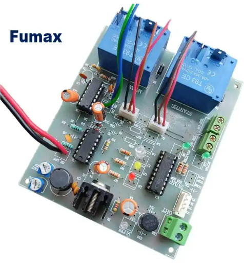
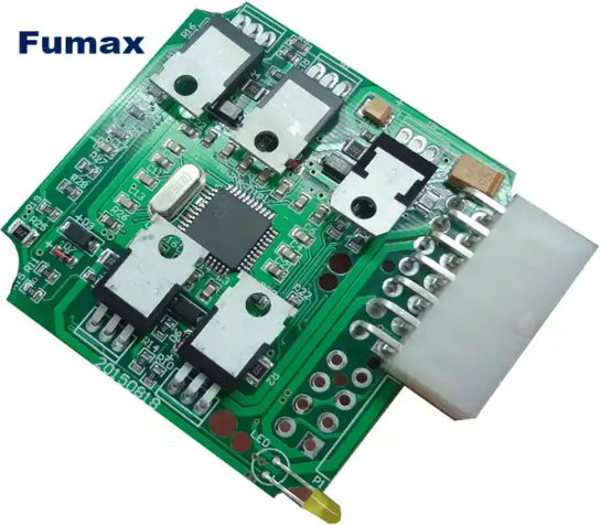
If you need to know about PCB multilayer boards manufactured by fumax, please contact us, we provide prototype PCB board manufacturing and PCB assembly services.
PCB multilayer board manufacturer
PCB multilayer board manufacturers refer to companies that specialize in the design, manufacturing and sales of PCB multilayer boards. These companies usually have advanced production equipment and manufacturing technology and can provide high-quality, high-reliability PCB multi-layer board products.
Shenzhen Fumax Technology Co., Ltd. is one of the largest PCB multi-layer board manufacturers in mainland China. It is engaged in the design and manufacturing of PCB multi-layer boards and provides PCB OEM/ODM services. Fumax has advanced production equipment and manufacturing technology and is able to provide high-quality, high-reliability PCB multi-layer board products.
The products produced by Fumax are widely used in communications, computers, automotive electronics, medical equipment and other fields. When choosing a PCB multilayer board manufacturer, you need to consider factors such as product quality, reliability, delivery cycle, and price.